Unwanted Radiation Countermeasures Explained in 20 Minutes
The following text was written for a different occasion, but since it contains content of high public value, I decided to extract it and publish it separately. I’ll write about things that might be useful, from how radiation occurs to hints for countermeasures to practical operation. The content leans fairly practical, so I’ve kept it fairly short (whether it’s a 20-minute read depends on the person). If you want the theoretical details of electromagnetism, consult a specialized textbook. The base of my knowledge of electromagnetism was mostly this textbook I used in university.
My practical experience with unwanted radiation countermeasures is largely based on my time at a certain major company. (I spent many days holed up in an anechoic chamber, over and over again…) The power supply circuits were often made in-house, and many products had PCB configurations built up as later additions, so it was a fairly troublesome category of product when it came to unwanted radiation countermeasures — I gained a lot of experience there.
First, about radiation
“Unwanted radiation” is also called “unintentional radiation.” Essentially it means radio waves are being emitted that weren’t intended to be emitted. So where does it come from? To a greater or lesser extent, it comes from “every corner of the electronic circuit.” That said, in a system where current flows cleanly, radiation hardly occurs at all. Here, “flowing cleanly” means going out and coming back cleanly.
Any signal is established as a system in which current supplied from the power source is converted into some form and sent out somewhere, and once it is caught at a distant point (this is where it’s read as a signal), that current returns to the power source through some other path. The selection of this system (which path the current flows through) is basically determined by wherever impedance is lowest. (The roots of this go down to quantum theory, actually — if you’re interested, it’s fun to study.) But on a typical PCB, current can’t go back and forth that cleanly (it gets forced to take detours, or reflects off dead ends), and imbalances occur in current density.
When I was in the Bay Area, I worked with an NVIDIA layout designer and saw his design — he skillfully used traces at subtle angles that were neither vertical (90 degrees), horizontal (0 degrees), nor diagonal (45 degrees) as commonly seen on typical PCBs, along with gently curved traces. This is a design consideration to minimize imbalances in current density and avoid creating wasteful L components or reflections.
When current density becomes imbalanced, some of the charge cannot return cleanly to the power source and jumps out looking for somewhere to go. Roughly speaking, this is the source of unwanted radiation. The charge that jumps out seeks a way back via the path of lowest impedance. The place expected to have the lowest impedance relative to the negative side of the power supply is usually GND. So if GND is nearby where there’s an imbalance in current density, the charge jumps there, and the radiation ends up dealt with at a very small level.
But if the impedance from GND to the power supply isn’t as low as expected, or there’s no effective GND nearby, the electric field lines go all the way around and out, and an electric field arises — in other words, unwanted radiation is observed. To prevent this, common techniques applied to GND include
- placing a large number of vias on the GND
- widening the GND area
- making an inner layer a solid GND plane
- placing GND on both sides of high-speed signals
Roughly speaking, all of these are measures to lower impedance and let the current return cleanly.
So, for now, what can be said about radiation is:
- It’s not emitted evenly across the whole board but stands out prominently from a specific location (often described as “blowing out” from there)
- Imbalances in current density are affected by all sorts of conditions, so honestly they’re hard to read
Hints for countermeasures
What can be done about unwanted radiation countermeasures hasn’t changed much, no matter how the times change — even in the age of AI and big data, even if the singularity arrives.
- Hit the source
- Strengthen power/GND countermeasures
- Assume radiation will occur and put a lid on the smell afterward
Hitting the source
The idea here is to hit the “source = the original oscillator or clock.” This is an extremely fundamental countermeasure, so if you can pull this off well, the countermeasure is completely finished.
Concretely, “hitting” means
- reducing harmonics
- reviewing traces and GND
The closer a signal gets to a square wave, the more harmonics appear in it. It’s common for a design with a 10MHz main clock to fail unwanted radiation testing at 20MHz or 30MHz. This is due to harmonics. Generally, the higher the frequency, the harder it is to deal with, so lower frequencies are always preferable. Dulling the waveform within an acceptable range can be an effective countermeasure.
Something similar happens when signal reflection (such as ringing) occurs due to impedance mismatch.
Also, because current density distribution is frequency-dependent when harmonics remain (since various impedances have frequency characteristics), it’s a common occurrence in unwanted radiation countermeasures to end up in a game of whack-a-mole, where hitting the 3rd harmonic causes the 5th to appear.
Concrete ideas for countermeasures:
- Insert RC (or LC) into clocks or high-speed signals
- Insert damping resistors or ferrite beads into clocks or high-speed signals (to prevent reflection)
When developing a product, it’s common to make a “clock table” — a summary of the frequencies of crystals or PLLs serving as sources, clocks used for communication, and so on. This becomes a clue when you actually tackle countermeasures.
Common examples generally include:
- USB (480MHz, 12MHz, etc.)
- SoC oscillators (tens of MHz)
- SDIO (~200MHz, etc.)
- Audio MCLK (24.576MHz, etc.) and so on.
In cases like this, it’s preferable to limit your thinking to “things that appear externally as signals.” Why? Because if that clock is blowing directly from the silicon itself, countermeasures can only be taken internally, and the noise is probably escaping externally via the power/GND path — so that’s where you should focus your hits.
Oscillator circuits
Places like oscillators are usually very simple in terms of circuitry. So what you need to watch for is
- whether the pattern is efficiently connected at the shortest distance
- whether the signal is going back and forth to other layers through vias
That’s about it. In other words, there isn’t much you can do here.
Also, when the generated clock is forced to take a long journey, it’s common to route it into an inner layer. This is a common countermeasure to strengthen it against noise by sandwiching it between GND layers. There’s some disagreement about this — I personally think there’s also merit to the view that if it’s kept on the surface, countermeasures become possible (like adding a damping resistor or a C to make a filter).
Communication circuits
I touched on communication clocks above, but if radiation does occur, USB is probably the toughest case. That’s because you want to keep the eye pattern clean for USB to guarantee communication performance. You can’t casually dull the signal — the simplest countermeasure is off the table. Conversely, there are also cases where the USB communication itself is noisy and radiation is blowing from there. In such cases, the root cause is almost always reflection, but suppressing reflection kills two birds with one stone: the waveform becomes cleaner and communication errors decrease, and unwanted radiation goes down. Checking the differential impedance with a TDR or similar might reveal where the reflection is occurring.
Communication systems very often consist of multiple signals with the same source and destination, so the signals usually run in parallel. Noise coupling tends to happen easily between signals running in parallel in general. Trouble can occur, for example, when noise gets coupled onto an analog signal (like audio) because a clock is running parallel to it. Same idea. If you keep in mind which high-speed signals should be somewhat guarded against, it’s preferable to keep them as far away as possible from noise-sensitive signals, or, if that’s difficult, to design the PCB so R or C can be inserted later.
Strengthening power/GND countermeasures
What you need to think about is how to return noise generated in the power supply or signals to GND as gently as possible.
Reviewing decoupling capacitor placement and values
In addition to the GND-strengthening measures already mentioned, reviewing the placement and values of decoupling capacitors is also a kind of GND-strengthening measure. Capacitor impedance has frequency characteristics — basically, smaller values pass high frequencies, and larger values don’t pass them as much. Roughly speaking, the former helps reduce AC-type noise, and the latter helps reduce DC-type noise.
If you already know which band is failing the unwanted radiation test, it’s sometimes effective to change values specifically targeting a smooth return to GND there. Changing impedance changes the current density distribution. An MCU, for example, often has multiple decoupling capacitors hanging off the same potential. Roughly speaking, such capacitors play two roles: supporting DC power supply, and lowering power supply impedance against high-frequency noise. This kind of decoupling capacitor is often connected right away to a large GND, so if this power supply is noisy, adjusting or adding decoupling capacitor values can sometimes lower the noise level.
Something in series with power/GND
Noise is current. So if you make it consume as heat through a resistor, the noise itself disappears. That said, carelessly increasing an impedance component that operates at frequencies used for DC or communication can cause operational problems. If the noise frequency is far higher than the communication frequency, inserting a filter or ferrite bead in series with the power/GND that sharply cuts that band can be very effective. When applying this idea, you also need to pay attention to whether the noise is coming from outside that power system or being generated internally. If it’s from outside, even if the noise frequency overlaps with the communication frequency, you can first cut it off sharply and then, within the power system, build a mechanism that covers short-term power supply through adjustment of decoupling capacitor values. Happy ending. At that point, you can think of the capacitor as being like a battery with an internal resistance that is frequency-dependent, called impedance. Smaller values are suited to short-term, small-quantity supply, and larger values are suited to medium- to long-term, large-quantity supply. The exact balance is a matter of cut and try. If the cause is noise from an AC adapter, USB bus power, or a switching power supply, hitting it there can be expected to bring things down quite a bit. It’s preferable to think mainly from the perspective of what to do at the device’s entry point. From the perspective of the power supply IC, on the other hand, it should be avoided as much as possible for each IC to get contaminated with noise and return it to the power supply IC side. Concretely, dropping it with an LC filter or similar is the simple solution. And when you think about which power rails tend to get contaminated, the ones that often come to mind are CPUs, memory buses, DSPs, FPGAs, GPUs, and so on.
Putting a lid on the smell
The last resort. This is about countermeasures after the fact.
Shielding
This is a method used in many communication modules. Naturally it also reduces noise, and it easily satisfies the Radio Act’s requirement for a “module” — that it be difficult to modify — so many modules come with shielding.
Sheet metal, if you can add it, is the strongest noise countermeasure component. But always ground that sheet metal to GND. Sheet metal left floating in potential acts as a new antenna or reflector. A classic example of skillfully using a reflector is the Yagi antenna.
Making cables twisted pair
Twisted pair is effective when noise generated somewhere is riding on the cable. A cable is fundamentally a very capable antenna. Noise riding on a cable usually goes somewhere and causes trouble, so it should be removed. Detailed explanations of the effect of twisted pair are widely available online, so I’ll leave that to those sources. Essentially, it’s the columbus’s-egg trick of making the electromotive forces generated on the cable by noise point in opposite directions at close range, so they cancel each other out.
Other last-ditch efforts
- Wrapping a ferrite core around the offending signal line
- Rerouting wiring (attaching and fixing it to sheet metal if available)
- Sticking on radio wave absorbing material here and there
- Electrically connecting a dirty GND to a point close to earth ground
These measures often work really well, but they tend to involve increased manual work or expensive countermeasure parts, and are often not preferable as a medium- to long-term solution. Honestly, it’s a dilemma.
What to do at the start of countermeasures
Given the ideas for countermeasures described above, what you should do at the start of countermeasures is clarify, as precisely as possible, what the source is for the frequency that’s failing. Units where clocks of similar frequency exist in multiple places require particular caution.
The steps are:
- Enumerate the frequencies present on the PCB and make an educated guess
- If it’s possible to stop it via software, try stopping the clock (clocking it down is also fine)
- If it can’t be stopped, cut off the circuit by removing the part, etc.
A handy tool in this process is a portable simple spectrum analyzer. I use this one (it’s cheap but surprisingly usable):
RF Explorer Spectrum Analyzer, Simplified Handheld Digital Pocket-Size Spectrum Analyzer (3G Combo)
Know-how for pinpointing the source location ① “Disassemble it”
If you’re using parts where stopping the clock isn’t easy, you may have no choice but to observe everything while operating together. With small devices, or when boards are close to each other, it may simply not be clear where the source is. In such cases, it’s effective to stretch out the cables and physically separate the boards. Take them out of the enclosure, line the boards up on a desk, and probe over them with the spectrum analyzer. Of course, this doesn’t guarantee a strictly identical state — it’s purely a method for pinpointing where the radio waves are blowing out from.
Know-how for pinpointing the source location ② “Probe directly with the spectrum analyzer”
A spectrum analyzer is generally understood to be something you attach an antenna to. That’s correct, but there’s also a different way to use it: you can attach a probe (you can view things normally this way). By directly probing components or GND with a probe, you can see disturbances in current density in quite fine detail. However, the important cautions are as follows.
- Use a probe made with high-frequency-capable coaxial cable
- Don’t probe the terminal directly — instead attach, for example, a 1pF leaded ceramic capacitor at the tip of the terminal and probe the component through that (because DC coming in will destroy the spectrum analyzer)
This might be a bit advanced.
Know-how for pinpointing the source location ③ “Touch it with your hand”
The human body is actually a rather capable noise countermeasure component (it has capacitance, and in many cases it’s grounded), and touching something with your hand can sometimes lower the observed radiation. If you find such a spot, that’s where the countermeasure should go. Similarly, sometimes just touching a cable lowers it, or touching two specific spots at the same time lowers it. These become major hints for countermeasures.
Cautions when pinpointing the source location
- Radio waves have polarization. If you don’t keep changing the antenna’s orientation and testing, you can overlook things
- Below 1GHz, you also need to worry about radiation in directions other than horizontal (radiation toward the floor). Above 1GHz, conversely, you don’t need to worry about anything other than horizontal
- Create a radio-quiet environment
What to think about after finding out where the radio waves are blowing from
Once you’ve found where the radiation is coming out, there are things you should think through carefully before jumping straight to “okay, countermeasures!”
The location of the source of emission and the location of the origin
First, a very important point is whether the location where it’s blowing out and the location of the origin match.
If they match, the countermeasures available are quite limited. For example, if a processor’s internal clock is emitting directly from the processor, often the only option is shielding (metal or radio wave absorbing material). That said, this kind of case isn’t seen much in recent CPUs and GPUs — manufacturers have already dealt with it — so basically you just need to keep in mind that here, what you can do is very limited.
Communication path or power/GND
If it’s a communication path, you’re relatively in luck. It’s common, for example, for radio waves to blow out from FFC wiring. In that case, just wrapping copper foil tape around it as shielding can bring it down quite a bit. If it’s wiring on the PCB, just sticking on copper foil grounded to GND or a radio wave absorbing sheet can fix it neatly. In these cases, immediate countermeasures are relatively easy, but since the processing is labor-intensive or costly, I think you should eventually fix the PCB. For cable wiring, for example, building an RC or LC filter around the connector or inserting a countermeasure component like a common mode choke could make it disappear cleanly, and for PCB wiring, arranging guard GND or inner-layer GND properly could resolve it. The most troublesome case is when it’s blowing from the power/GND system.
It seems to be coming from a wide range (multiple locations), and the power or GND plane is the culprit
When it’s coming from the plane, it’s truly troublesome, for these reasons:
- Hitting one spot usually causes another spot to pop up (a whack-a-mole situation, taking time to deal with)
- If your investigation has reached this point, it’s likely a pattern where the source couldn’t be hit, and additionally it wasn’t coming from any one specific easy-to-hit spot. In that case, the only options left are to “spread it out” or “seal it off”
“Spreading it out” means dispersing the noise as much as possible: creating a tight connection structure for power and GND, as already described above, so that current flows as cleanly as possible. There’s no magic bullet that solves this in one shot — it becomes steady, patient work (whack-a-mole).
Simulation has traditionally been used to avoid this whack-a-mole situation.
Murata’s Femtet is a fairly monstrous solution, yet very reasonably priced. https://www.muratasoftware.com/
“Sealing it off” is, again, the “put a lid on the smell” already mentioned. There’s nothing particular to add.
As a bit of a curveball, there’s also the technique of deliberately creating an imbalance and hitting it there. Concretely, this means separating power/GND from each other at high frequency as much as possible. Doing so limits where the noise can go, and lets you hit it there — that’s the idea. However, doing this on a small PCB weakens each power/GND, which can leave you with no more moves and stuck. It’s quite tricky.
Summary
Unwanted radiation countermeasures are often constrained by the stage, schedule, budget, and so on. If you have plenty of time and budget, remaking the PCB is the proper approach. Running a simulation at that stage isn’t a bad idea either (ideally you’d do it from the start, but it’s hard to make time for it unless the risk has already materialized). If you anticipated the risk in advance — for example, if you’re carrying over the design of a board or module that gave you trouble before — I’ve also on several occasions thrown in 0Ω resistors just about everywhere I could think of. Then, once radiation testing actually fails, you swap those out for countermeasure parts. So, honestly, most of the cases where you end up racking your brain over unwanted radiation countermeasures are ones without this kind of margin or advance planning (of course they are). That leads to a tendency toward “let’s just stick stuff on everywhere for now and see what happens!” (I did that plenty of times myself when I was starting out), but I think knowing the principles and overall picture described up to this point can be useful in many ways.
- Stick things properly where the radio waves are actually emitting (is it the plane? the cable?)
- Change what you stick on depending on whether you’re turning the noise into heat or returning it to GND
- If you’re aiming for shielding through GND expansion, be careful not to create a place where current density spikes oddly
And so on. The countermeasure work itself will involve some amount of groping around, but there’s a huge difference between groping around with this kind of knowledge in your head versus fumbling in the dark.
Bonus
L or R
If you’re going to insert something in series to suppress noise, the options that come up are L (ferrite bead, etc.) or R (resistor). Because L has frequency characteristics, it fits very well with the purpose of cutting a specific frequency. R itself can become a source of DC-type voltage drop, so at first glance it seems difficult to use.
However, when you use L in series, whether intended or not, and regardless of whether there’s a decoupling capacitor present, an LC filter is formed. That’s because the input capacitance of the IC where the L was inserted, the capacitance of the PCB, and various other C’s are always attached. The frequency characteristics of an LC filter always show a resonance characteristic.
This means that at some point, the filter can actually work to strengthen the noise (series resonance). A point you intended to weaken at one location ends up becoming stronger at another location. The technique to mitigate this effect is the ferrite bead. Take, for example, this Murata item: https://www.murata.com/ja-jp/api/pdfdownloadapi?cate=cgsubChipFerriBead&partno=BLM03AG102SN1%23 whose impedance characteristic looks like this.
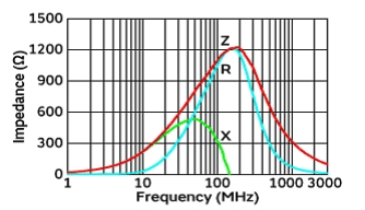
If you bring this frequency close to the resonant frequency (by choosing the right ferrite bead), the combined effect lets you cleanly bring down the target frequency. Think it through properly, and bring it down properly. R, by contrast, can be thought of very simply — just calculate the cutoff frequency and build an RC filter, and the noise will come down quite obediently. But being obedient is all it can offer — you can’t do anything special with it, like creating a peak at a specific location. Learn the advantages and disadvantages of each and use them skillfully.
Sequential handling across production lots
It’s a common story to handle countermeasures sequentially across production lots. You can probably easily imagine a situation like: the first lot ships next month, so the only countermeasure available is radio wave absorbing material, but there’s about half a year until the second lot, so proper countermeasures can be taken by then. In that case, it might be good to form two teams if possible (maybe two people in charge), since what needs to be done differs so much. Short-term whack-a-mole is a brute-force endurance match. Long-term countermeasures, on the other hand, are an approach of solving things in one or two shots through proper calculation (including simulation) and redoing prototypes, relying on careful thought rather than sheer number of attempts. Skillfully combining both approaches, with an eye to timing, is what I’d call the know-how of the development field.
Originally published in Japanese at https://clazytech.com/2020/10/364/. Translated with LLM assistance and reviewed before publication.